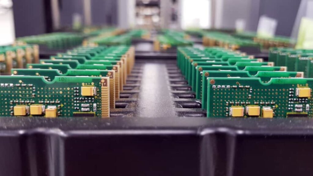
Printed Circuit Boards form the heart of a modern electronic device and are at that critical juncture, acting as the backbone of an electronic component system by interconnecting all the hardware. PCBs are the most crucial product created through a complex process of manufacturing where raw materials are transformed into sophisticated electronic interconnection systems.
PCB Manufacturing Explained: Preparation of Raw Material
Manufacturing of PCBs starts with careful selection and preparation of base materials. FR-4 is the most utilised substrate-a rigid fibreglass material that has very good mechanical and electrical insulation characteristics. The substrate is a material made by impregnating epoxy resin into woven fibreglass cloth for excellent strength in structure and thermal stability. 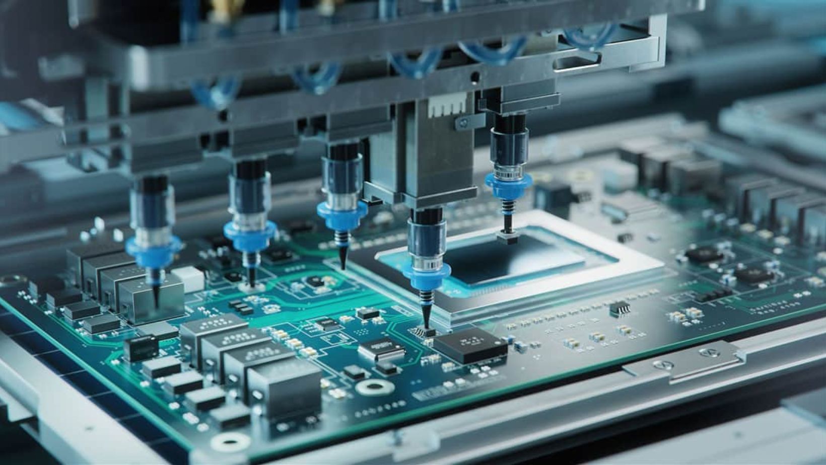
PCB Manufacturing Explained: Circuit-Image Transfer Design
Electrical engineers create detailed designs for the circuits using specific CAD programs before actual manufacturing. The digital blueprint pre-defines the precise positioning of copper traces, component locations, and interconnect paths. Extensive verification is carried out through design rule checks and simulation to ensure functionality in terms of electrical performance and also manufacturability. The image transfer stage is critical in which the transferred design has been put onto the copper-clad substrate. This is done by a photolithographic process similar to complex printing processes. A photosensitive layer referred to as the photoresist is applied with care to the copper surface. Then, the circuit design is projected onto that layer using strong UV light to selectively harden the resistor in areas corresponding to the circuit pattern. Areas unexposed will remain soft and can therefore be removed chemically, effectively creating a well-desired stencil for subsequent copper etching.
PCB Manufacturing Explained: Etching and Circuit Formation
Copper etching is a precision chemical process that removes unwanted copper and leaves the intricate circuit traces designed by engineers. Immediately following the photoresist development, the panel is submerged into a controlled chemical bath containing ferric chloride or other specialised etching solutions. The chemicals dissolve unprotected copper, selectively revealing the exact circuit pathways. The process must be precisely controlled in terms of the chemical concentration, temperature, and the time of immersion to achieve spotless, correct definition of the circuit traces. Modern manufacturers of PCBs use increasingly advanced techniques such as laser direct imaging and additive manufacturing processes that lay down copper only where it is needed, reducing the amount of chemicals wasted and enhancing environmental sustainability. These emerging technologies enable increasingly complex and miniaturised circuit designs with tolerances measured in micrometres.
PCB Manufacturing Explained: Layer Alignment and Lamination
Most modern electronic devices require multi-layer PCBs in which several circuit layers are aligned in a stack. Each layer is manufactured separately and then registered to others using complex systems for alignment. Specialised registration holes and optical alignment techniques ensure that the circuit layers match with microscopic precision, generally within 25-50 micrometres. In the lamination process, these layers are bonded together with the help of heat and extreme pressure. Prepreg materials: these materials contain thin layers of partially cured epoxy resin sandwiched between copper layers for electrical insulation as well as mechanical bonding. Industrial hydraulic presses apply controlled temperatures around 180°C and pressures up to 400 pounds per square inch, which provides uniform bonding and excludes the possibility of air gaps that may lead to circuit malfunctioning.
PCB Manufacturing Explained: Drilling and Via Formation
There are a number of holes, called vias, which can electrically connect different layers of a PCB. Modern PCB manufacturing uses computer-controlled drilling machines to create thousands of tiny microscopic holes with extraordinary precision. Drill bits, often made from tungsten carbide, can fabricate holes as small as 0.1 mm in diameter, thus making designs increasingly dense and complex. 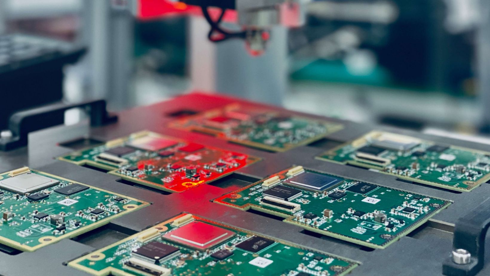
PCB Manufacturing Explained: Surface Finishing and Protection
Protective and functional surface finishes are applied in the final stages of manufacturing. These coatings serve a number of purposes: protection of exposed copper from oxidation, providing solderable surfaces, and enhancing the overall durability of the board. The common surface finishes include HASL (Hot Air Solder Levelling), ENIG (Electroless Nickel Immersion Gold), and some other advanced versions like immersion silver or organic solderability preservatives. Each finish has its special merits: HASL has excellent solderability and is low in cost, while ENIG offers superior flatness and corrosion resistance, making it ideal for fine-pitch components and demanding electronic applications. The choice is based on particular design requirements, expected operation conditions, and device performance that can be foreseen.
PCB Manufacturing Explained: Quality Control and Testing
Rigorous quality control at perhaps the final most critical stage of manufacture involves high-resolution cameras combined with advanced machine learning algorithms. It will also find microscopic defects which no human eye could ever detect. Automated Optical Inspection-AOI and X-ray inspection technologies guarantee that every circuit trace, via, and connection meet the most strict quality standards. Electrical testing verifies that the functional performance of the board is correct, subjecting each PCB to a simulated operating condition. Flying probe testers make use of several precision probes in testing every electrical connection for continuity, resistance and signal integrity. Some manufacturers also choose to conduct environmental stress testing by exposing boards to temperature cycling, humidity, and mechanical shock to ensure reliability under extreme conditions. This refined PCB manufacturing process lays a strong foundation for integrating embedded firmware development services, ensuring seamless hardware-software interaction in advanced electronic systems.
In Conclusion
As electronic devices further get miniaturised, intensified, and made more complex, PCB manufacturing technologies will continue to evolve and make available possibilities not previously considered in systems of electronic interconnection.


